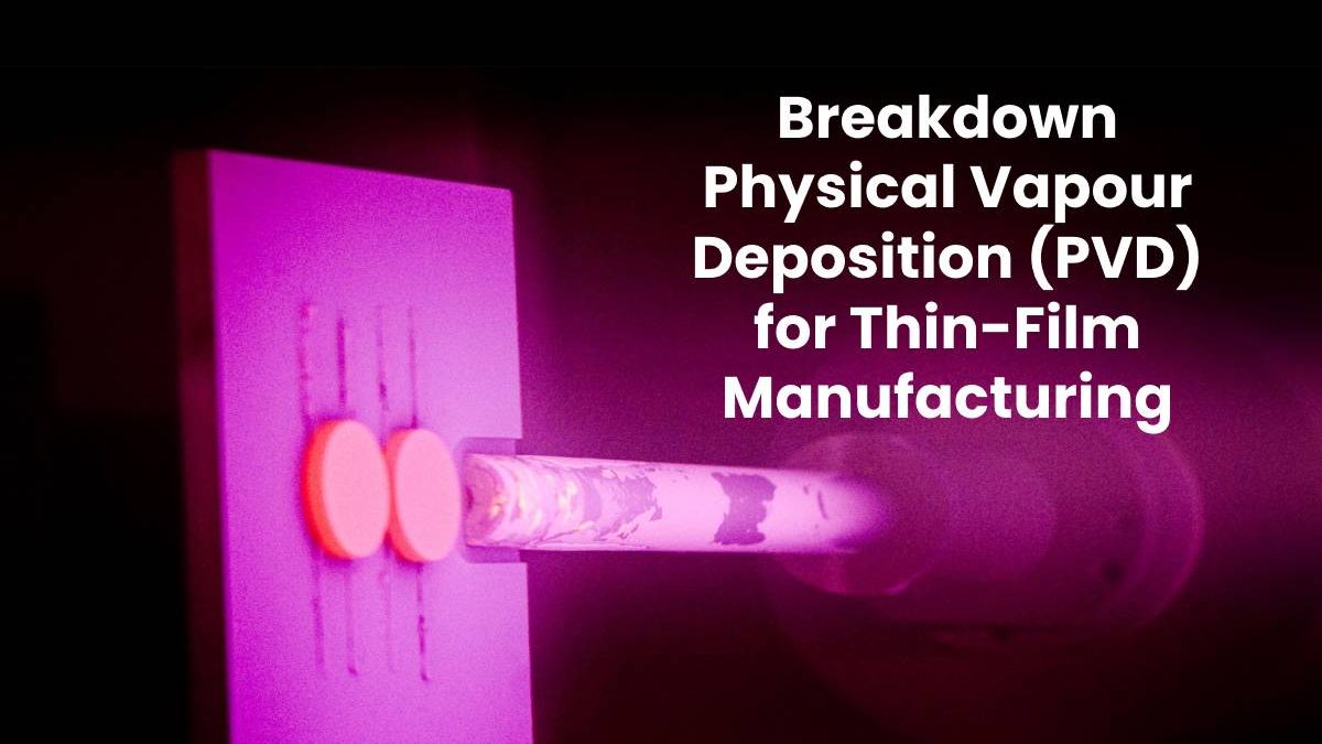
A Breakdown of Physical Vapour Deposition (PVD) for Thin-Film Manufacturing
PVD (physical vapour deposition) coating is a type of thin-film deposition technique that vaporises target material in a vacuum chamber and deposits it on a substrate surface. A PVD coating may consist either of pure materials or alloy compositions.
Physical vapour deposition is a high-precision method that enables the atomic-level application of the coating material. PVD coatings form an indispensable part of microchips, durable protective films, optical lenses, solar panels, and various medical devices.
Keep reading to find out how physical vapour deposition works to produce pure, top-performing PVD coatings.
What’s PVD, and How Is It Applied?
Physical vapour deposition methods use two main techniques: thermal evaporation and sputtering. In thermal evaporation, the solid material becomes vaporised as it reaches a boiling point in a vacuum chamber. The vapour stream rises and condenses on the substrate.
In sputtering, the coating material receives a high-energy charge that dislocates atoms and molecules, which then land on the substrate and coat it with an even, precise layer of thin film.
Common PVD thin-film applications include computer chips, LED displays, durable protective layers, and chrome, gold, or platinum plating over another metal like stainless steel.
The Physical Vapour Deposition Process in Thin-Film Manufacturing
Physical vapour deposition can form atomic- and molecular-level thin films. The most common deposition coating method is arc ion plating, which involves four basic steps:
- Vacuum exhaust. The high vacuum chamber pumps oxygen, water vapour, and impurities out through an exhaust port.
- Heating. Heating removes any remaining impurities and moisture clinging to the substrate surface.
- Etching. Argon ions from a plasma source impact the surface with force and remove any oxides or impurities.
- Coating. A cathodic arc forms between the chamber and the target material. The charge vaporises the target material into a plasma state, turning neutral atoms into positive ions. Under a negative voltage current, the substrate attracts these ions, which form a high-precision film on the substrate surface.
Depending on the processing conditions and coating material, a PVD coating can improve the heat resistance, strength, durability, and performance of many devices across diverse industries. Precise technologies enable near-perfect control of film thickness and purity.
High-adhesion PVD coatings offer many benefits, such as:
- Improving wear resistance in metalworking tools
- Creating optical coatings and filters
- Forming reflective films for decorative displays
PVD systems work in applications across multiple industries, including the automotive, aerospace, chemical, marine, nuclear, and medical fields.
Korvus Technology uses the physical vapour deposition process in its HEX series, a modular thin film deposition system with multiple uses such as sputter deposition, contact metallisation, EM sample preparation, and research of new PVD coating types.
Final Thoughts
PVD coating technologies can improve resistance to wear, heat, erosion, hardiness, sliding properties, and other variables in many tools and devices. Physical vapour deposition creates thin films with superb reflective, optical, and conductive functions.
Semiconductor thin films are employed in several computer hardware nowadays, being responsible for a great part of the advances in processing power, cloud computing, and more.
As PVD technology continues to evolve, multiple industries are using these methods to achieve higher performance and lower production costs. Very likely, the future of computing will be shaped by thin film technology.
Related posts
Sidebar
Recent Posts
An Inside Look Of Paraulogic
Introduction Welcome to the exciting world of Paraulogic! Are you ready to dive into a linguistic adventure and put your…
Empowering Artists with Cryptocurrency: A Guide to Selling Art Using NFTs
In the ever-evolving landscape of the art world, artists are constantly seeking innovative ways to showcase and monetize their creations….


